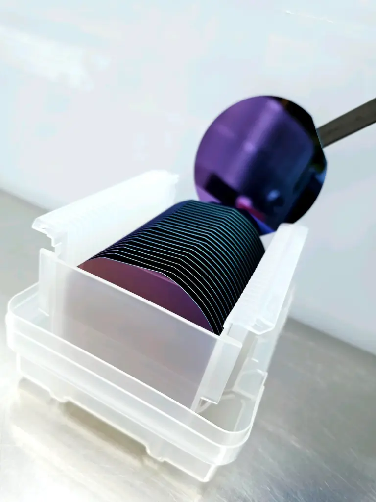
PRD1027 - 2,000A Wet Thermal Oxide/2,000A Std LPCVD Nitride
Two-layer film stack on silicon: 0.2um (2,000A) of wet thermal silicon dioxide (SiO2) grown first, followed by 0.2um (2,000A) of stoichiometric LPCVD silicon nitride (Si3N4). Substrates are cleaned in our class 100 cleanroom before processing. This is a furnace process, so oxide is grown on both surfaces of the wafer. Film stress is 800 MPa tensile or greater, with a refractive index of 2.00 +/- 0.05 at 632.8 nm. 100mm (4 inch) diameter wafers. Ships with a film Certificate of Conformance.
Need something different? Email sales@roguevalleymicro.com for a quote.
| -Material: Silicon |
| -Diameter: 100mm |
| -Type/Dopant: P/Boron |
| -Orientation: <100> |
| -Resistivity: >1 ohm-cm |
| -Thickness - W: 525+/-25um |
| -Surface Prep: SSP |
| -Flat/Notch: Flat, Semi Standard |
| -Film Type: Wet Thermal Oxide, Stoichiometric LPCVD Nitride |
| -Film Thickness: 2,000A +/-5%, 2,000A +/-5% |
| -Film Stress: ≥800 MPa Tensile |
| -Sides Processed: Both |
| -Quantity: 1 lot = 25 wafers |